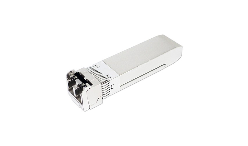
SFP+ 10Gbps (40KM)
10G SFP+ LR (ER-1310/ER-1550) Transceiver


SFP+ 10Gbps (40KM)
10G SFP+ LR (ER-1310/ER-1550) Transceiver
SFP+ 10Gbps (40KM)
10G SFP+ LR (ER-1310/ER-1550) Transceiver
OVERVIEW
10GBase-LR/LW Small Form Factor Pluggable SFP+ transceivers are compliant with the current SFP+ Multi-Source Agreement (MSA) Specification. The high performance uncooled 1310nm DFB/1550nm EML transmitter and high sensitivity PIN receiver provide superior performance for 10GBASE-LR/LW applications up to SMF 40km optical links.
FEATURES
- Compliant with IEEE802.3ae 10GBASE-LR/LW
- Compliant with CPRI Option 7, 8
- Compliant with SFF-8431 SFP+ MSA
- Support 8.5Gb/s to 11.32Gb/s Multi-Rate
- Hot Pluggable
- 1310nm DFB/1550nm EML laser transmitter
- Duplex LC connector
- 2-wire interface for management and diagnostic monitor compliant with SFF-8472
- Single +3.3V power supply
- Link distance 40km over SM fiber
- RoHS Compliant
SPECIFICATIONS
Absolute Maximum Ratings
Parameter
|Symbol
|Min.
|Max.
|Unit
|Note
| | --- | --- | --- | --- | --- | --- | |Storage Temperature
|Ts
|-40
|+85
|°C
|| |
Supply Voltage
|Vcc
|-0.5
|+4.0
|V
|| |
Storage Relative Humidity
|RH
|5
|95
|%
|| |
Operational Humidity
|RH
|0
|85
|%
||
Recommended Operating Conditions
Parameter
|Symbol
|Min.
|Typ.
|Max.
|Unit
|Note
| | --- | --- | --- | --- | --- | --- | --- | |Case Operating Temperature
|Top
|0
||
+70
|°C
|| |
Case Operating Temperature (-E model)
|Top
|-40
||
+85
|°C
|| |
Supply Voltage
|Vcc
|+3.13
|+3.3
|+3.47
|V
|| |
Supply Current
|Icc
||
|
350
|mA
|| |
Supply Current (-E model)
|Icc
||
|
380
|mA
||
Transmitter Electro-Optical Characteristics
VCC= 3.13V to 3.47V, TOP = 0 °C to 70 °C (standard model); TOP = -40 °C to 85 °C (-E model)
Parameters
|Symbol
|Min.
|Typ.
| |Max.
|Unit
|Note
| | --- | --- | --- | --- | --- | --- | --- | --- | |Operating Date Rate
|DR
|8.5
|10.3125
| |11.32
|Gb/s
|| |
Optical Launch Power
|Po
|0
|| |
+4
|dBm
|1
| |Optical Center Wavelength
|λc
|1260
|1310
| |1355
|nm
|| |
Spectral Width (-20dB)
|△λ
||
| |
1
|nm
|| |
Side Mode Suppression Ratio
|SMSR
|30
|| |
|
dB
|| |
Optical Extinction Ratio
|ER
|3.5
|| |
|
dB
|| |
Optical Eye Mask
||
IEEE802.3ae
| | | | || |
Relative Intensity Noise
|RIN
|| |
|
-128
|dB/Hz
|| |
Differential Data Input Swing
|VIN
|180
| ||
850
|mV
|| |
TX Disable Input Voltage-Low (TX ON)
|TDISVL
|GND
| ||
0.8
|V
|| |
TX Disable Input Voltage-High (TX OFF)
|TDISVH
|2.0
| ||
Vcc
|V
|| |
TX Fault Output Voltage-Low (TX Normal)
|TFLTVL
|GND
| ||
0.8
|V
|| |
TX Fault Output Voltage-High (TX Fault)
|TFLTVH
|2.0
| ||
Vcc
|V
||
Notes: 1. The optical power is launched into a 9/125μm single-mode fiber
Receiver Electro-Optical Characteristics
VCC= 3.13V to 3.47V, TOP = 0 °C to 70 °C (standard model); TOP = -40 °C to 85 °C (-E model)
Parameters
|Symbol
|Min.
|Typ.
|Max.
|Unit
|Note
| | --- | --- | --- | --- | --- | --- | --- | |Operating Date Rate
|DR
|8.5
|10.3125
|11.32
|Gb/s
|| |
Receiver Sensitivity
|PIN_min
||
|
-16
|dBm
|1
| |Maximum Input Power
|PIN_max
|+0.5
||
|
dBm
|1
| |Optical Center Wavelength
|λC
|1260
||
1620
|nm
|| |
LOS De-Assert
|LOSD
||
|
-17
|dBm
|| |
LOS Assert
|LOSA
|-30
||
|
dBm
|| |
LOS Hysteresis
|LOSHY
|0.5
||
|
dB
|| |
Differential data output voltage
|Vout
|300
||
900
|mV
|| |
Receiver LOS Signal Output Voltage-Low
|LOSVL
|GND
||
0.8
|V
|| |
Receiver LOS Signal Output Voltage-High
|LOSVH
|2.0
||
Vcc
|V
||
Note1: Measured with a PRBS 231-1 test pattern @10.3125Gbps BER<10-12
Pin Assignment

Diagram of Host Board Connector Block Pin Numbers and Name
Pin Description
Pin
|Name
|Function / Description
| | --- | --- | --- | |1
|VeeT
|Transmitter Ground
| |2
|TX_Fault
|Transmitter Fault Indication (1)
| |3
|TX_Disable
|Transmitter Disable – Turns off transmitter laser output (2)
| |4
|SDA
|2-wire Serial Interface Data Line (SDA: Serial Data Signal) (3)
| |5
|SCL
|2-wire Serial Interface Clock (SCL: Serial Clock Signal) (3)
| |6
|Mod_ABS
|Module Absent, connected to VeeT or VeeR in the module (3)
| |7
|RS0
|Rate Select 0, optional (5)
| |8
|Rx_LOS
|Receiver Loss of Signal Indication (4)
| |9
|RS1
|Rate Select 1, optional (5)
| |10
|VeeR
|Receiver Ground
| |11
|VeeR
|Receiver Ground
| |12
|RD-
|Receiver Inverted Data output, AC coupled
| |13
|RD+
|Receiver Non-Inverted Data output, AC coupled
| |14
|VeeR
|Receiver Ground
| |15
|VccR
|Receiver 3.3V Power Supply
| |16
|VccT
|Transmitter 3.3V Power Supply
| |17
|VeeT
|Transmitter Ground
| |18
|TD+
|Transmitter Non-Inverted Data Input, AC coupled
| |19
|TD-
|Transmitter Inverted Data Input, AC coupled
| |20
|VeeT
|Transmitter Ground
|Note1: TX Fault is open collector/drain output which should be pulled up externally with a 4.7K~10KΩ resistor on the host board to supply <VccT+0.3V or VccR+0.3V. When high, this output indicates a laser fault of some kind. Low indicates normal operation. In the low state, the output will be pulled to <0.8V.
Note2: TX Disable input is used to shut down the laser output per the state table below. It is pulled up within the module with a 4.7K~10KΩ resistor. 1) Low(0~0.8V): Transmitter on; 2) Between(0.8V and 2V): Undefined; 3) High (2.0~ VccT): Transmitter Disabled; 4) Open: Transmitter Disabled.
Note3: These are the module definition pins. They should be pulled up with a 4.7K~10KΩ resistor on the host board to supply less than VccT+0.3V or VccR+0.3V. MOD_ABS is grounded by the module to indicate that the module is present.
Note4: Rx_LOS (Loss of signal) is an open collector/drain output which should be pulled up externally with a 4.7K~10KΩ resistor on the host board to supply <VccT+0.3V or VccR+0.3V. When high, this output indicates the received optical power is below the worst case receiver sensitivity (as defined by the standard in use). Low indicates normal operation. In the low state, the output will be pulled to <0.8V.
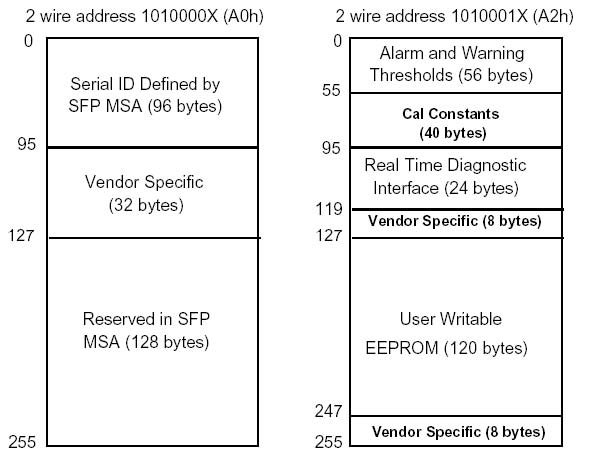
Digital Diagnostic Functions
As defined by the SFP MSA (SFF-8472) Lantech’s SFP transceivers provide digital diagnostic functions via a 2-wire serial interface, which allows real-time access to the following operating parameters:
- Transceiver temperature
- Laser bias current
- Transmitted optical power
- Received optical power
- Transceiver supply voltage
It also provides a sophisticated system of alarm and warning flags, which may be used to alert end-users when particular operating parameters are outside of a factory-set normal range.
The operating and diagnostics information is monitored and reported by a Digital Diagnostics Controller (DDC) inside the transceiver, which is accessed through the 2-wire serial interface. When the serial protocol is activated, the serial clock signal (SCL pin) is generated by the host. The positive edge clocks data into the SFP+ transceiver into those segments of its memory map that are not write-protected. The negative edge clocks data from the SFP+ transceiver. The serial data signal (SDA pin) is bi-directional for serial data transfer. The host uses SDA in conjunction with SCL to mark the start and end of serial protocol activation. The memories are organized as a series of 8-bit data words that can be addressed individually or sequentially.
For more detailed information including memory map definitions, please see the SFP MSA (SFF-8472) Specification.
Digital Diagnostic Memory Map
Digital Diagnostic Monitoring Characteristics Map
Parameter
|Accuracy
|Unit
|Note
| | --- | --- | --- | --- | |Temperature
|±3
|℃
|Internal Calibration
| |Supply Voltage
|±0.1
|V
|Internal Calibration
| |TX Bias Current
|±5
|mA
|Internal Calibration
| |TX Output Power
|±3
|dB
|Internal Calibration
| |RX Received Optical Power
|±3
|dB
|Internal Calibration
|
ORDERING INFORMATION
NOTE: Distances are indicative only. To calculate a more precise link budget based on specific conditions in your application, please refer to the optical characteristics.
Part Number
|TX
|RX
|Link
|DDM
|Mode
|Temp.
| | --- | --- | --- | --- | --- | --- | --- | |8330-225D-V1
|1310nm
|1260nm~1620nm
|40km
|Yes
|Single-mode
|0~70°C
| |8330-225DE-V1
|1310nm
|1260nm~1620nm
|40km
|Yes
|Single-mode
|-40~85°C
| |8330-205D-V1
|1550nm
|1260nm~1620nm
|40km
|Yes
|Single-mode
|0~70°C
| |8330-205DE-V1
|1550nm
|1260nm~1620nm
|40km
|Yes
|Single-mode
|-40~85°C
|