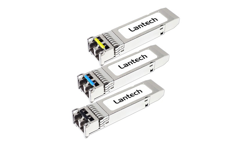
SFP 2.5Gbps (2KM)
1310nm FP, Duplex LC, 2.5GBase-X SFP Transceiver


SFP 2.5Gbps (2KM)
1310nm FP, Duplex LC, 2.5GBase-X SFP Transceiver
SFP 2.5Gbps (2KM)
1310nm FP, Duplex LC, 2.5GBase-X SFP Transceiver
OVERVIEW
Lantech 2.5GBase-X Small Form Factor Pluggable SFP transceivers are compliant with the current SFP Multi-Source Agreement (MSA) Specification. The high performance 1310nm FP transmitter and high sensitive PIN receiver provide superior performance for SONET/SDH applications up to 2km optical links with single mode fiber.
FEATURES
- Compliant with SONET OC-48 SR and SDH STM-16 I16 Standard
- Compliant with 2500Base-X
- Compliant with SFP MSA
- Compliant with SFP8472 diagnostic monitoring interface
- Hot Pluggable
- 1310nm FP laser transmitter
- Duplex LC connector
- 2-wire interface for management and diagnostic monitor
- Single +3.3V power supply
- Transmission distance of 2km over single mode fiber
- RoHS Compliant
SPECIFICATIONS
Absolute Maximum Ratings
Parameter
|Symbol
|Min.
|Max.
|Unit
|Note
| | --- | --- | --- | --- | --- | --- | |Storage Temperature
|TST
|-40
|+85
|°C
|| |
Supply Voltage
|Vcc
|-0.5
|4.0
|V
|| |
Storage Relative Humidity
|RH
|5
|95
|%
||
Recommended Operating Conditions
Parameter
|Symbol
|Min.
|Typ.
|Max.
|Unit
|Note
| | --- | --- | --- | --- | --- | --- | --- | |Case Operating Temperature
(Standard model)
TOP
|-10
||
70
|°C
|| |
Case Operating Temperature
(-E model)
TOP
|-40
||
85
|°C
|| |
Supply Voltage
|Vcc
|+3.15
|+3.3
|+3.45
|V
|| |
Supply Current
|ICC
||
200
|260
|mA
||
Transmitter Electro-Optical Characteristics
Parameter
|Symbol
|Min.
|Typ.
|Max.
|Unit
|Note
| | --- | --- | --- | --- | --- | --- | --- | |Optical launch Power
|PO
|-10
||
-3
|dBm
|1
| |Center Wavelength
|λC
|1280
|1310
|1340
|nm
|| |
Spectral Width (RMS)
|Δλ
||
|
2
|nm
|| |
Optical Extinction Ratio
|ER
|8.2
||
|
dB
|| |
Rise/Fall Time (10%~90%)
|Tr/Tf
||
|
0.16
|ns
|| |
Optical Eye Mask
||
ITU-T G.957 STM-16
| | | || |
Differential Data Input Voltage
|VDIFF
|300
||
1600
|mV
|| |
Transmit Disable Voltage
|VDIS
|2.0
||
Vcc
|V
|| |
Transmit Enable Voltage
|VEN
|GND
||
GND+0.8
|V
||
Notes: 1. The optical power is launched into a 9/125μm single-mode fiber.
Receiver Electro-Optical Characteristics
Parameter
|Symbol
|Min.
|Typ.
|Max.
|Unit
|Note
| | --- | --- | --- | --- | --- | --- | --- | |Receiver Sensitivity
|PINMIN
||
|
-18
|dBm
|1
| |Maximum Input Power
|PINMAX
|-3
||
|
dBm
|1
| |Operating Center Wavelength
|λC
|1100
||
1610
|nm
|| |
LOS De-Assert
|LOSD
||
|
-18
|dBm
|| |
LOS Assert
|LOSA
|-30
||
|
dBm
|| |
LOS Hysteresis
|LOSVHY
|0.5
||
|
dB
|| |
Differential Data Output Voltage
|Vout, pp
|300
||
1000
|mV
|| |
Data Output Rise/Fall Time (10%~90%)
|Tr/Tf
||
|
0.18
|ns
|| |
Receiver LOS Signal Output Voltage-Low
|LOSVL
|GND
||
GND+0.5
|V
|| |
Receiver LOS Signal Output Voltage-High
|LOSVH
|2.4
||
Vcc
|V
||
Notes: 1. Measured with a PRBS 231-1 test pattern @ 2488Mbps BER < 10-10
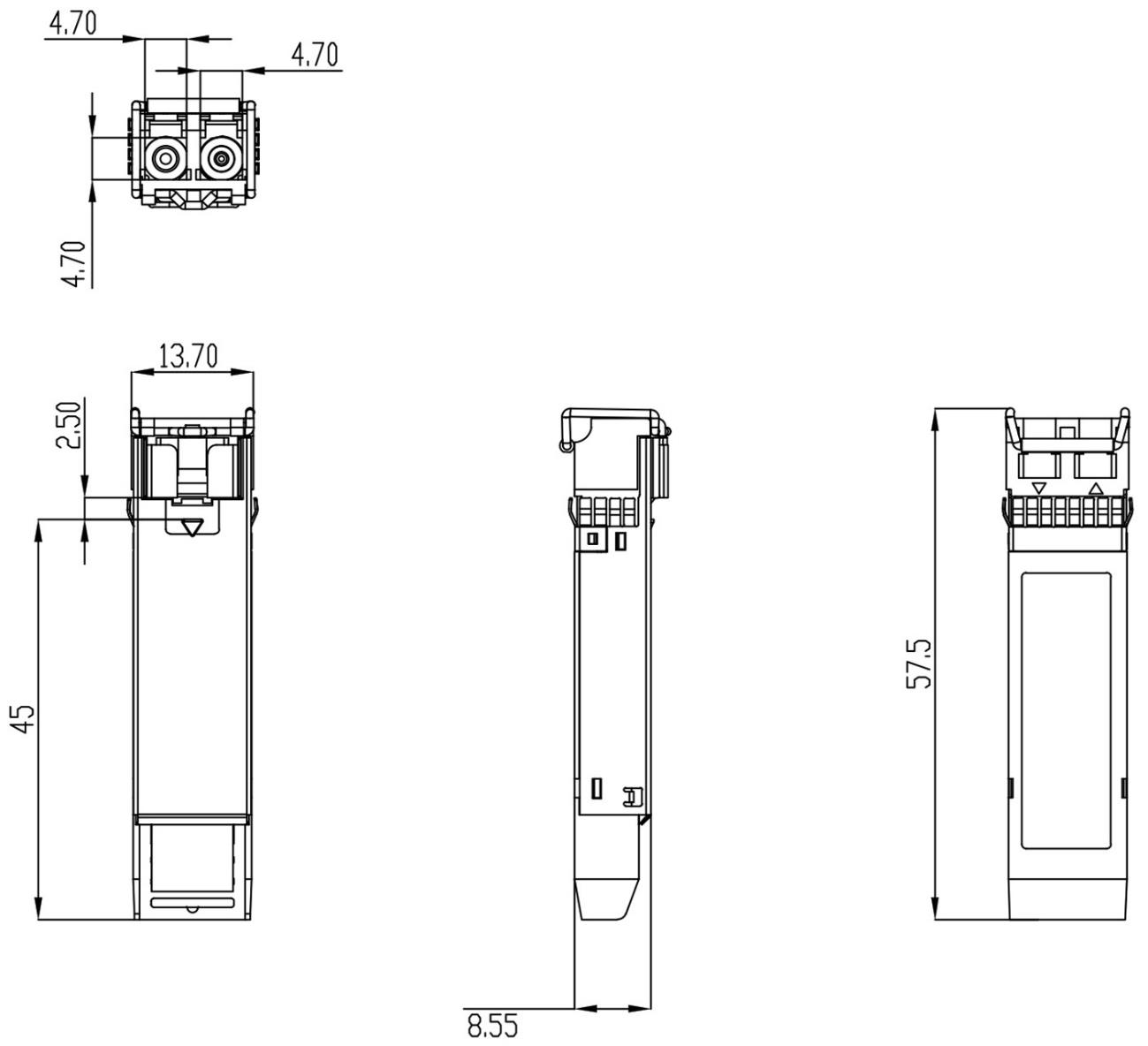
Pin Assignment

Diagram of Host Board Connector Block Pin Numbers and Name
Pin Description
Pin
|Name
|Function / Description
| | --- | --- | --- | |1
|VeeT
|Transmitter Ground
| |2
|TX_Fault
|Transmitter Fault Indication (1)
| |3
|TX_Disable
|Transmission Disable – Module disables on high or open (2)
| |4
|MOD-DEF(2)
|Module Definition 2 – SDA: Serial Data Signal
| |5
|MOD-DEF(1)
|Module Definition 1 – SCL: Serial Clock Signal
| |6
|MOD-DEF(0)
|Module Definition 0 – LVTTL Low (3)
| |7
|Rate Select
|Not Connected – Open Circuit
| |8
|LOS
|Receiver Loss of Signal (4)
| |9
|VeeR
|Receiver Ground
| |10
|VeeR
|Receiver Ground
| |11
|VeeR
|Receiver Ground
| |12
|RD-
|Inverse Received Data out, Differential LVPECL, AC coupled
| |13
|RD+
|Received Data out, Differential LVPECL, AC coupled
| |14
|VeeR
|Receiver Ground
| |15
|VccR
|Receiver Power
| |16
|VccT
|Transmitter Power
| |17
|VeeT
|Transmitter Ground
| |18
|TD+
|Transmitter Data In, Differential LVPECL, AC coupled
| |19
|TD-
|Inverse Transmitter Data In, Differential LVPECL, AC coupled
| |20
|VeeT
|Transmitter Ground
|Note1: TX Fault is open collector/drain output which should be pulled up externally with a 4.7K~ 10KΩ resistor on the host board to supply <VccT+0.3V or VccR+0.3V. When high, this output indicates a laser fault of some kind. Low indicates normal operation. In the low state, the output will be pulled to <0.8V.
Note2: TX Disable input is used to shut down the laser output per the state table below. It is pulled up within the module with a 4.7K~10KΩ resistor. 1)Low(0~0.8V): Transmitter on; 2)Between(0.8V and 2V): Undefined; 3)High (2.0~ VccT): Transmitter Disabled; 4)Open: Transmitter Disabled
Note3: Mod-DEF 0, 1, 2. These are the module definition pins. They should be pulled up with a 4.7K~10KΩ resistor on the host board to supply less than VccT+0.3V or VccR+0.3V. Mod-DEF(0) is grounded by the module to indicate that the module is present. Mod-DEF(1) is clock line of two wire serial interface for optional serial ID. Mod-DEF(2) is data line of two wire serial interface for optional serial ID.
Note4: LOS (Loss of signal) is an open collector/drain output which should be pulled up externally with a 4.7K~10KΩ resistor on the host board to supply <VccT+0.3V or VccR+0.3V. When high, this output indicates the received optical power is below the worst case receiver sensitivity (as defined by the standard in use). Low indicates normal operation. In the low state, the output will be pulled to <0.8V.
ORDERING INFORMATION
Part Number
|TX
|Link
|Mode
|Temp.
| | --- | --- | --- | --- | --- | |8330-263D-V1
|1310nm
|2KM
|Single-mode
|-10~70°C
| |8330-263DE-V1
|1310nm
|2KM
|Single-mode
|-40~85°C
| All SFP P/N# ended with D are with DDM function